The Pixel 9 reportedly gears up for satellite SOS support
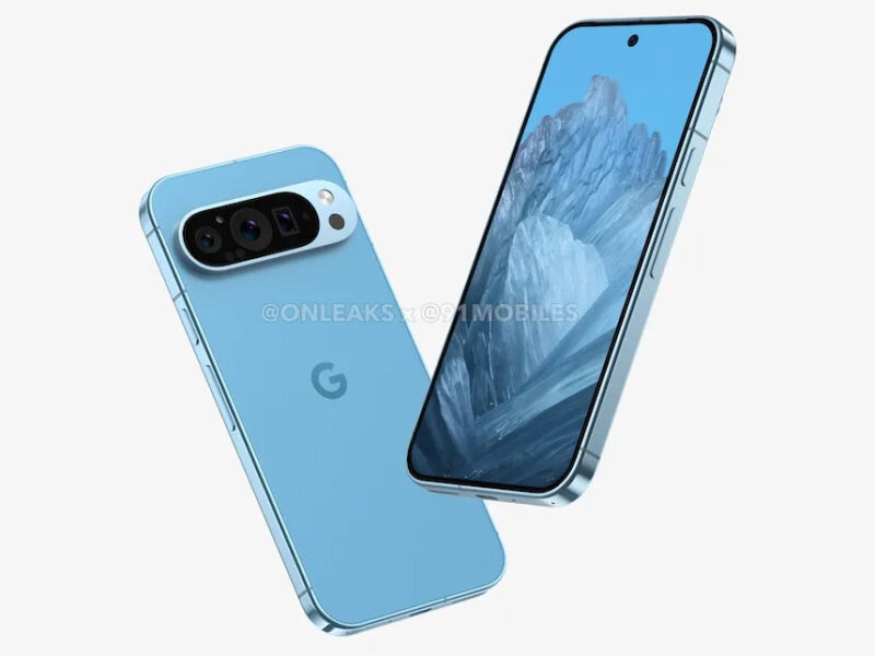
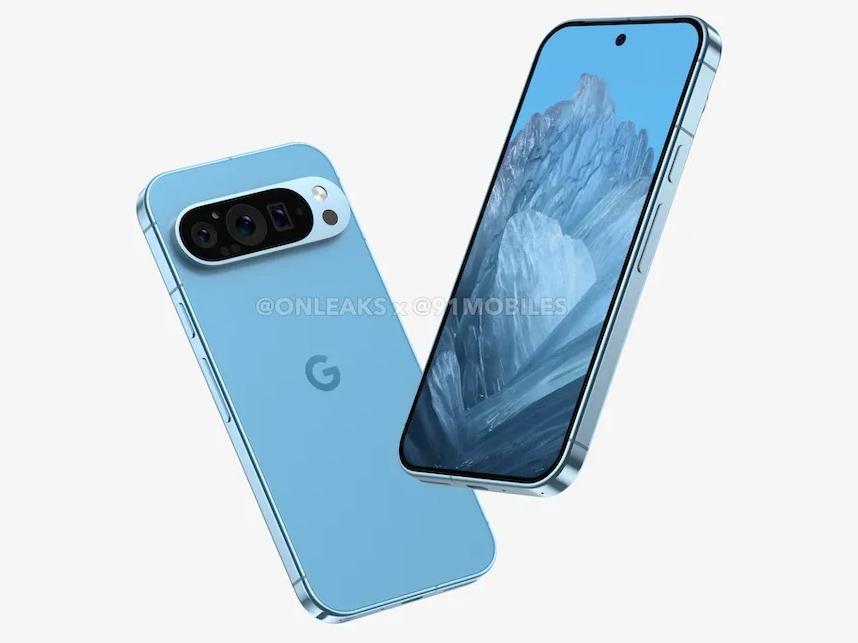
The smaller Pixel 9, with three cameras?!
Enlarge / The smaller Pixel 9, with three cameras?!

Google has been doing a lot of work in Android to support satellite-based messaging, and it sure would be nice if someone actually shipped some hardware it could use. Despite the feature launching with the iPhone 14 in 2022, Android manufacturers haven’t been super receptive to copying the idea of satellite messaging. Qualcomm and satellite company Iridium built a working solution and incorporated it into Qualcomm’s Snapdragon chips, only for zero Android manufacturers to support the feature, leading to the dissolution of the partnership. If Google wants an Android satellite SMS phone to play with, it seems like it will need to build the device itself.

Reliable leaker Kamila Wojciechowska over at Android Authority says Google is working on doing just that. It looks like the Pixel 9 will be getting emergency satellite SOS. Since the Pixel 6, Pixel phones have been the rare devices that don’t use Qualcomm modems. Google partners with Samsung and bases its Pixel Tensor chips on Samsung Exynos chips, and that means using Samsung’s (usually much maligned) modems, too. Citing a source, Wojciechowska says the Pixel 9 would use the new Exynos Modem 5400, along with its optional NTN (non-terrestrial network) capabilities, allowing the phone to be “the first to support Android’s native satellite implementation.” The initial service provider would be T-Mobile (just like the good old days).

The move would make sense. The whole original point of the Nexus/Pixel line was to give Google something to build Android on. By incorporating the latest hardware features into the next Pixel, Android gets a target to program for and test on. Otherwise, we’d have a chicken-and-egg problem where no one makes the hardware because there’s no software support, and no one makes software because there’s no hardware to program for. Google just does it all at once.

As for who would be powering T-Mobile’s satellite network, the company has a high-profile partnership with SpaceX, but those are LTE towers in space and work on regular devices with no special software (the recent demo was on a regular set of iPhones). The whole point of Android’s satellite implementation is dealing with traditional satellite problems like aiming at a far-away satellite, compressing the message a ton to actually make it to the satellite, and dealing with an unreliable connection. That’s not really relevant to the SpaceX partnership since that is trying to be a next-generation solution of “regular LTE in space,” designed around the world’s largest rocket and satellite network.

We’re just speculating here, but a better target for a “current-generation” system would be Skylo, which resells service from traditional satellite companies like Viasat and Inmarsat, so it would need all that aiming and unreliable connection software. In a wild coincidence, Skylo already has a press release out saying it has certified the Samsung Exynos Modem 5400 for use on its network. Skylo already has a relationship with T-Mobile, and the company powered the Motorola Satellite Link hotspot.

https://arstechnica.com/?p=2017214


Framework’s software and firmware have been a mess, but it’s working on them

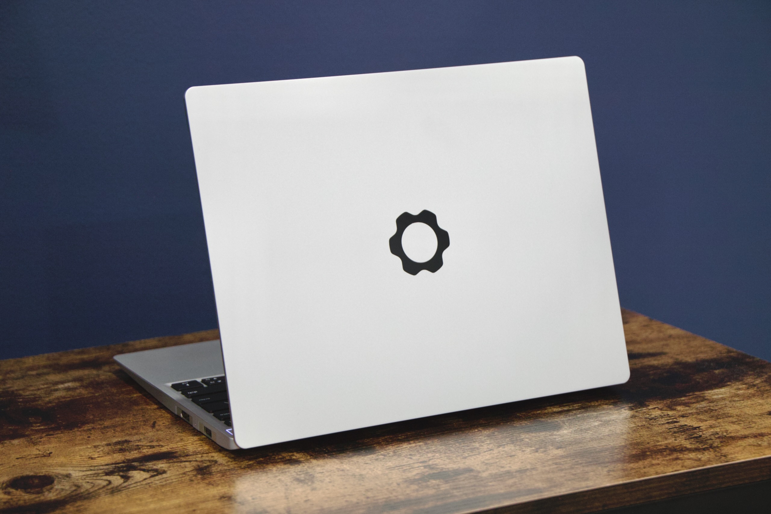
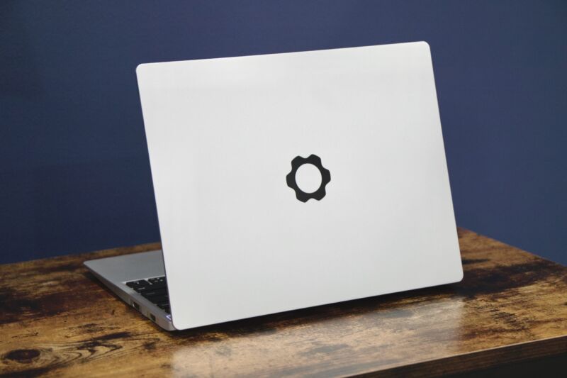
The Framework Laptop 13.
Enlarge / The Framework Laptop 13.
Andrew Cunningham

Since Framework showed off its first prototypes in February 2021, we’ve generally been fans of the company’s modular, repairable, upgradeable laptops.

Not that the company’s hardware releases to date have been perfect—each Framework Laptop 13 model has had quirks and flaws that range from minor to quite significant, and the Laptop 16’s upsides struggle to balance its downsides. But the hardware mostly does a good job of functioning as a regular laptop while being much more tinkerer-friendly than your typical MacBook, XPS, or ThinkPad.

But even as it builds new upgrades for its systems, expands sales of refurbished and B-stock hardware as budget options, and promotes the re-use of its products via external enclosures, Framework has struggled with the other side of computing longevity and sustainability: providing up-to-date software.

Driver bundles remain un-updated for years after their initial release. BIOS updates go through long and confusing beta processes, keeping users from getting feature improvements, bug fixes, and security updates. In its community support forums, Framework employees, including founder and CEO Nirav Patel, have acknowledged these issues and promised fixes but have remained inconsistent and vague about actual timelines.

But according to Patel, the company is working on fixing these issues, and it has taken some steps to address them. We spoke to him about the causes of and the solutions to these issues, and the company’s approach to the software side of its efforts to promote repairability and upgradeability.

Promises made

Here’s a case in point: the 12th-generation Intel version of the Framework Laptop 13, which prompted me to start monitoring Framework’s software and firmware updates in the first place.

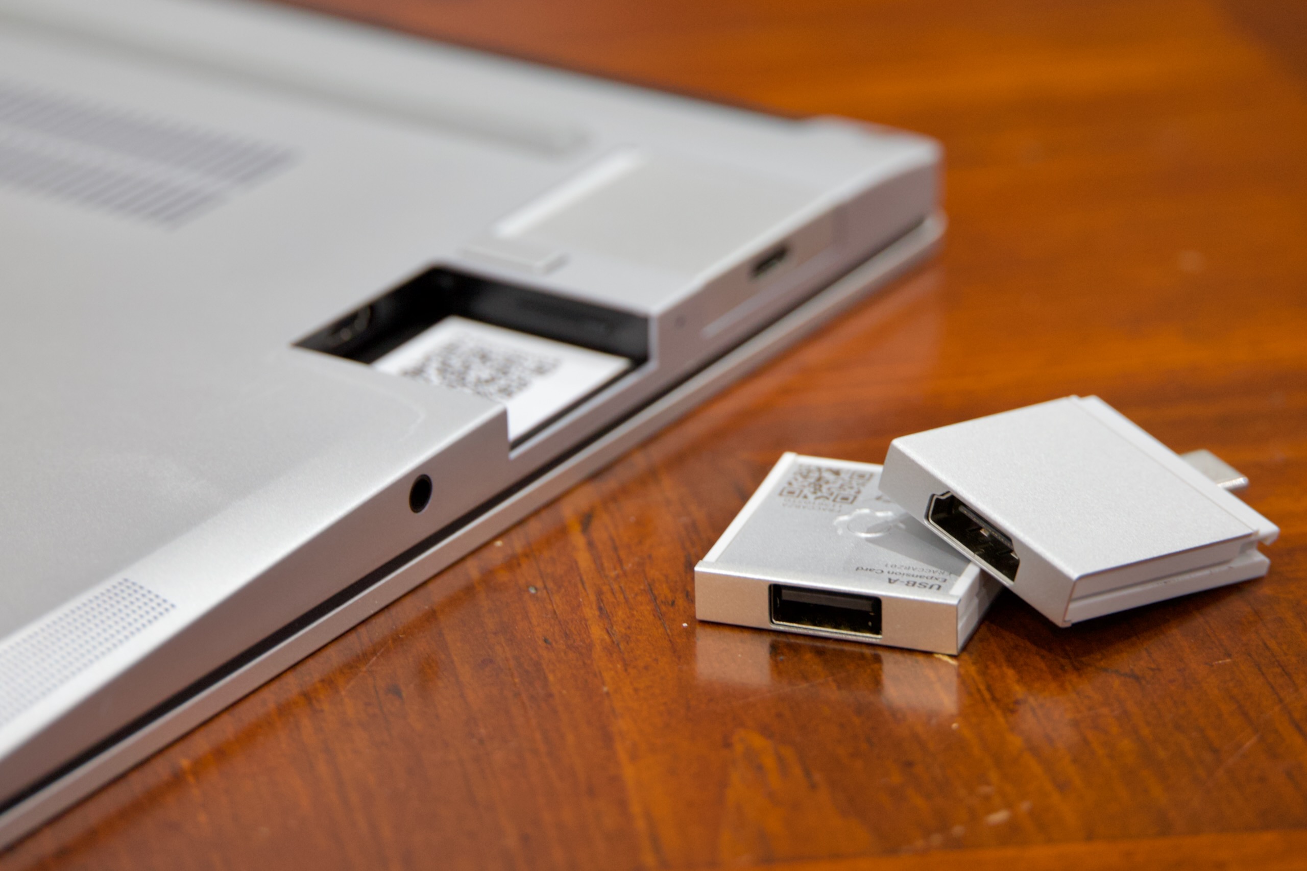
In November 2022, Patel announced that this model, then the latest version, was getting a nice, free-of-charge spec bump. All four of the laptop’s recessed USB-C ports would now become full-speed Thunderbolt ports. This wasn’t a dramatic functional change, especially for people who were mostly using those ports for basic Framework expansion modules like USB-A or HDMI, but the upgrade opened the door to high-speed external accessories, and all it would need was a BIOS update.

The recessed USB-C ports in the 12th-gen Intel version of the Framework Laptop 13 can be upgraded to fully certified Thunderbolt ports, but only if you're willing to install one in a long series of still-in-testing beta BIOSes.
Enlarge / The recessed USB-C ports in the 12th-gen Intel version of the Framework Laptop 13 can be upgraded to fully certified Thunderbolt ports, but only if you’re willing to install one in a long series of still-in-testing beta BIOSes.
Andrew Cunningham

A final version of this BIOS update finally showed up this week, nearly a year and a half later. Up until last week, Framework’s support page for that 12th-gen Intel laptop still said that there was “no new BIOS available” for a laptop that began shipping in the summer of 2022. This factory-installed BIOS, version 3.04, also didn’t include fixes for the LogoFAIL UEFI security vulnerability or any other firmware-based security patches that have cropped up in the last year and a half.

And it’s not just that the updates don’t come out in a timely way; the company has been bad about estimating when they might come out. That old12th-gen Framework BIOS also didn’t support the 61 WHr battery that the company released in early 2023 alongside the 13th-gen Intel refresh. Framework originally told me that BIOS update would be out in May of 2023. A battery-supporting update for the 11th-gen Intel version was also promised in May 2023; it came out this past January.

Framework has been trying, but it keeps running into issues. A beta 3.06 BIOS update with the promised improvements for the 12th-gen Intel Framework Laptop was posted back in December of 2022, but a final version was never released. The newer 3.08 BIOS beta entered testing in January 2024 but still gave users some problems. Users would go for weeks or months without any communication from anyone at Framework.

The result is multiple long forum threads of frustrated users asking for updates, interspersed with not-untrue but unsatisfying responses from Framework employees (some version of “we’re a small company” is one of the most common).

https://arstechnica.com/?p=2012352


SD cards finally expected to hit 4TB in 2025

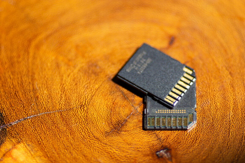
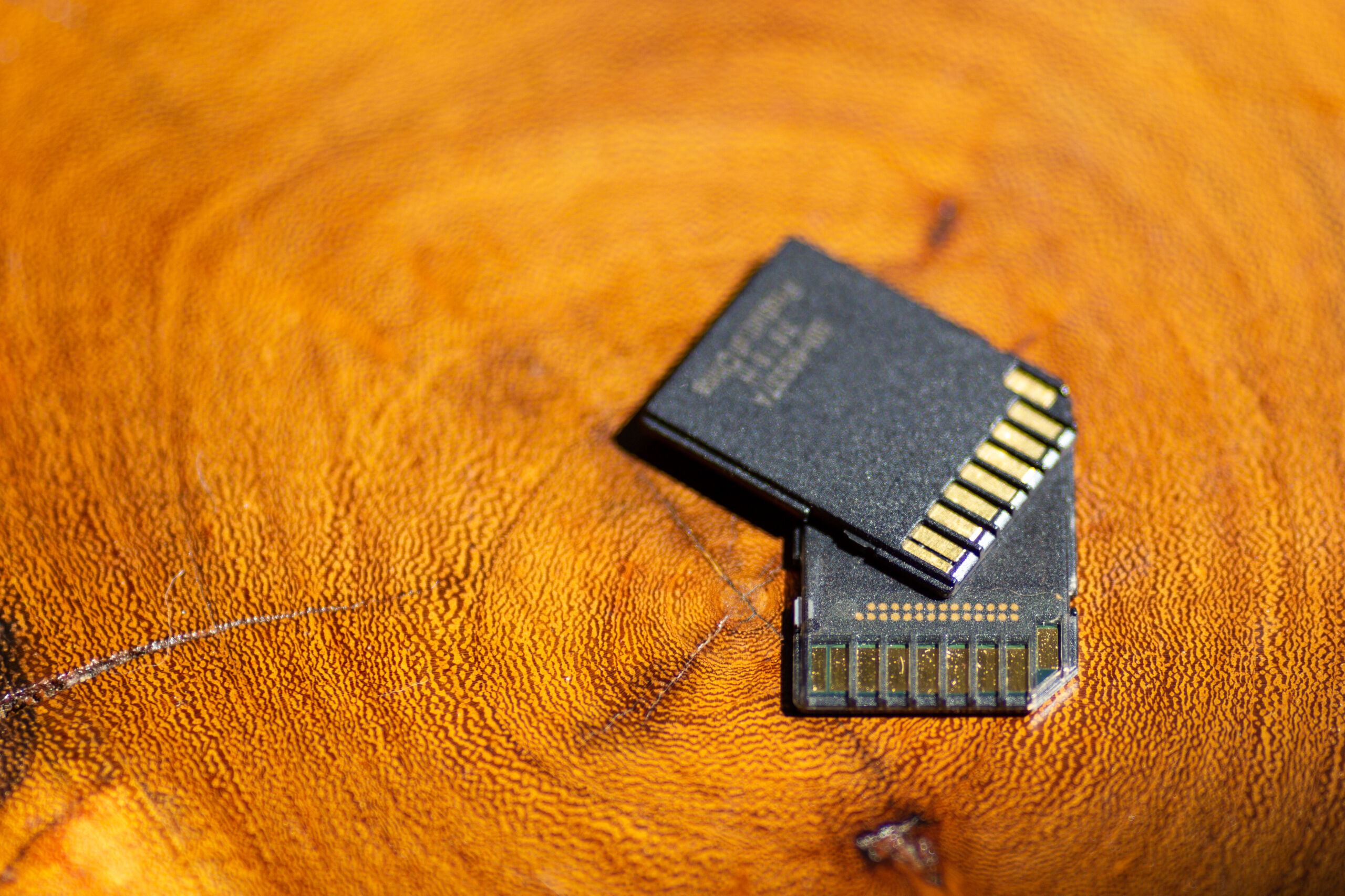
Two SD cards on a wood surface
Enlarge / Generic, non-Western Digital SD cards.

Western Digital plans to release the first 4TB SD card next year. On Thursday, the storage firm announced plans to demo the product in person next week.

Western Digital will launch the SD card, which follows the SD Association’s Secure Digital Ultra Capacity (SDUC) standard, under its SanDisk brand and market it toward “complex media and entertainment workflows,” such as high-resolution video with high framerates, using cameras and laptops, the announcement said.

The spacious card will use the Ultra High Speed-1 (UHS-1) bus interface, supporting max theoretical transfer rates of up to 104 MB per second. It will support minimum write speeds of 10 MB/s, AnandTech reported. Minimum sequential write speeds are expected to reach 30 MB/s, the publication said.

With those specs, the upcoming SD card should be able to fit storage-hungry video formats, including 8K, although the card won’t be speedy enough to support raw 8K video recording. That helps explain why Western Digital is initially previewing the offering at The National Association of Broadcasters’ annual event for broadcast and media professionals, which starts tomorrow in Las Vegas.

“Attendees will get a preview of the 4TB SD card’s full capacity and learn more about how it will expand the creative possibilities for cameras and laptops,” Western Digital said.

Hopefully, Western Digital will provide more information about the SD card at the event, as this week’s announcement didn’t go into further details, such as the type of NAND the card will use or whether it will support the SanDisk-created DDR200/DDR208 mode, which could enable higher data transfer speeds of up to 170 MB/s (but only with a host that supports that mode).

Western Digital didn’t say what the SD card would cost, but with its advanced capabilities and targeted audience of professional creators, the offering will likely have premium pricing. The 1TB SanDisk Extreme Pro SDXC UHS-I Card currently has a $140 MSRP.

WD’s announcement comes six years after the SD Association, which writes SD standards, announced the SDUC standard that bumped the max possible capacity for SD cards from 2TB to 128TB. As with many releases of new standards, some were eager to believe that “SD cards could soon hold 128TB of storage.” But with 4TB not expected to arrive until 2025 (assuming there are no delays), “soon,” even today, is unrealistic. The 2018 standard only made such capacities a possibility. At the time, the max theoretical capacities for an SD card had been 2TB for about nine years, but the most spacious SD cards actually available for purchase at the time were 512GB.

Today, the highest capacity SD cards readily available are 1TB (Western Digital also this week announced plans to release a 2TB SanDisk Extreme Pro SDXC UHS-I memory card at an unspecified date), while 2TB microSD cards only became available this year.

With Western Digital’s announcement, the industry inches closer to SD cards’ maximum potential. For professionals with high-storage needs, that’s exciting news, as having more capable technology opens more possibiltiies, like working with high-res media.

However, Western Digital’s announcement also comes as SanDisk’s reputation for reliable storage is in serious question by professional and long-time customers. There are multiple lawsuits about SanDisk Extreme portable SSDs reportedly failing unexpectedly. These alleged failures, combined with frustration around Western Digital’s limited response to reported data losses, could have professionals with work-critical storage needs consider waiting for another brand to make the leap to 4TB.

https://arstechnica.com/?p=2016986


The DiskMantler violently shakes hard drives for better rare-earth recovery

From magnets we came, to magnets we return.
Enlarge / From magnets we came, to magnets we return.
Garner Products

There is the mental image that most people have of electronics recycling, and then there is the reality, which is shredding.

Less than 20 percent of e-waste even makes it to recycling. That which does is, if not acquired through IT asset disposition (ITAD) or spotted by a worker who sees some value, heads into the shredder for raw metals extraction. If you’ve ever toured an electronics recycling facility, you can see for yourself how much of your stuff eventually gets chewed into little bits, whether due to design, to unprofitable reuse markets, or sheer volume concerns.

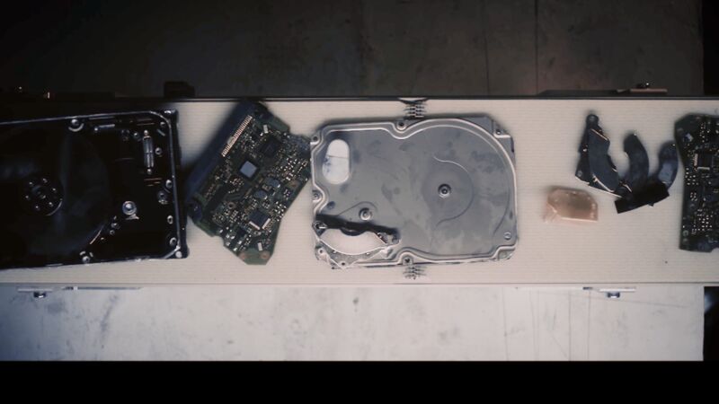
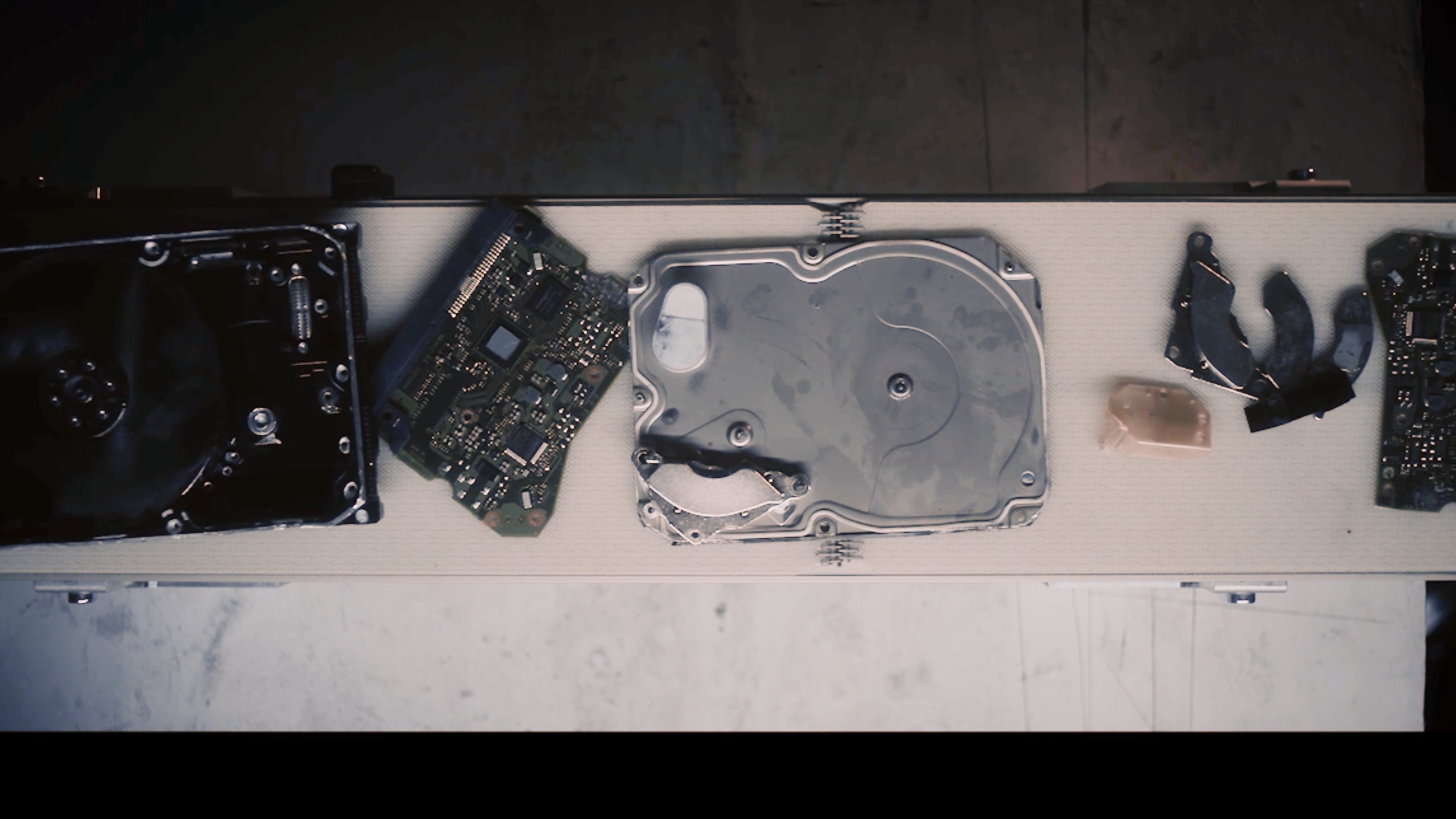
Traditional hard drives have some valuable things inside them—case, cover, circuit boards, drive assemblies, actuators, and rare-earth magnets—but only if they avoid the gnashing teeth. That’s where the DiskMantler comes in. Garner Products, a data elimination firm, has a machine that it claims can process 500 hard drives (the HDD kind) per day in a way that leaves a drive separated into those useful components. And the DiskMantler does this by shaking the thing to death (video).

The DiskMantler, using “shock, harmonics, and vibration,” vibrates most drives into pieces in between 8–90 seconds, depending on how much separation you want. Welded helium drives take about two minutes. The basic science for how this works came from Gerhard Junker, the perfectly named German scientist who fully explored the power of vibrations, or “shear loading perpendicular to the fastener axis,” to loosen screws and other fasteners.

As Garner’s chief global development officer, Michael Harstrick, told E-Scrap News, the device came about when a client needed a way to extract circuit boards from drives fastened with proprietary screw heads. Prying or other destruction would have been too disruptive and potentially damaging. After testing different power levels and durations, Garner arrived at a harmonic vibration device that can take apart pretty much any drive, even those with more welding than screws. “They still come apart,” Harstrick told E-Scrap News. “It just takes a little bit.”

Improving the recovery and sorting ease of hard drives is itself a useful thing, but the potential for rare-earth magnet recycling is particularly attractive. Most rare-earth magnet recycling involves “long-loop” recycling, or breaking them down into rare earth elements and then putting those back into the magnet production stream, which is energy-intensive and not very cost-effective. Electric vehicles and wind turbines have huge amounts of rare-earth magnets in them but rarely see recycling. Hard drives, while individually small, are massive in scale, with roughly 259 million shipped in 2021.

One Canadian firm, based on a University of Birmingham-patented process, wants to reuse drive magnets more directly, creating new sources that don’t require extraction and aren’t quite so globally concentrated. That Canadian firm, HyProMag, uses robotics to find and extract drives’ permanent magnets, then sends the rest of the disk off for recycling.

The technology is not all there yet, but soon enough, it looks like something interesting will shake out.

https://arstechnica.com/?p=2016916


Google kills “One” VPN service, says “people simply weren’t using it”

Google kills “One” VPN service, says “people simply weren’t using it”
Aurich Lawson

Another day, another dead Google product. The Google One VPN service we complained about last week is headed to the chopping block. Google’s support documents haven’t been updated yet, but Android Authority reported on an email going out to Google One users informing them of the shutdown. 9to5Google also got confirmation of the shutdown from Google.

The Google One VPN launched in 2020 as a bonus feature for paying Google One subscribers. Google One is Google’s cloud storage subscription plan that allows users to buy extra storage for Gmail, Drive, and Google Photos. In 2020, the plan was exclusive to the expensive 2TB tier for $10 a month, but later, it was brought down to all Google One tiers, including the entry-level $2-per-month option.

By our count, Google has three VPN products, though “products” might be too strong a word since they are all essentially the same thing—VPN market segments? There’s the general Google One VPN for Android, iOS, Windows, and Mac—this is the one that’s dying. There’s also the “Pixel VPN by Google One,” which came with Pixel phones (the “Google One” branding here makes no sense since you didn’t have to subscribe to Google One) and the Google Fi VPN that’s exclusive to Google Fi Android and iOS customers.

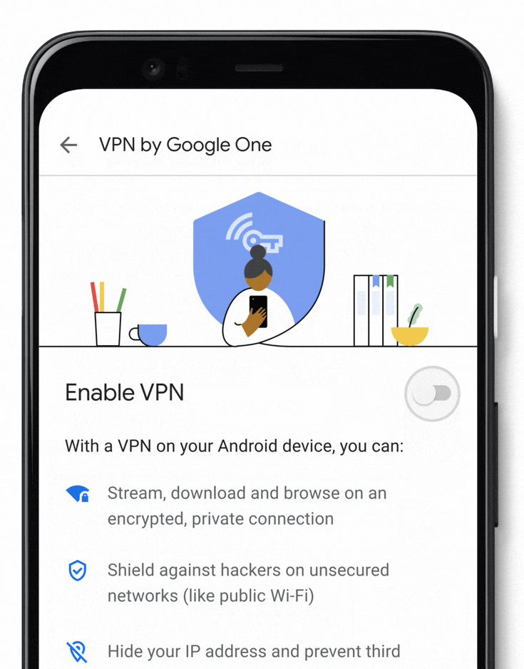
The Google One VPN settings.
Enlarge / The Google One VPN settings.

The Google One VPN that’s shutting down was by far the most flexible, with the widest platform support, and its shutdown represents Google ending VPN support for Windows and Mac. The Pixel and Fi VPNs will keep running, possibly with new branding.

A Google spokesperson told 9to5Google the Google One VPN is shutting down because “people simply weren’t using it.” The Windows client was also super buggy, and it’s probably easier to shut it down rather than fix it. There’s no shutdown date yet, but a message on this page says the VPN will be phased out “later in 2024.”

https://arstechnica.com/?p=2016925


TSMC’s $65 billion bet still leaves US missing piece of chip puzzle

President Biden speaking at the official opening of TSMC’s first Arizona fabrication plant in December 2022. The Taiwanese chipmaker plans to start manufacturing 2-nanometer chips in the US in 2028.
Enlarge / President Biden speaking at the official opening of TSMC’s first Arizona fabrication plant in December 2022. The Taiwanese chipmaker plans to start manufacturing 2-nanometer chips in the US in 2028.
Caitlin O’Hara/Bloomberg via Getty

Taiwan Semiconductor Manufacturing Company’s decision to bring its latest technology to America is a big step forward for US President Joe Biden’s quest for security in the vital tech supply chain—but still leaves Washington short of being able to completely produce the most complex chips in the US.

The world’s biggest chipmaker by sales must also pull off an intricate balancing act as it steps up its US presence, satisfying customers such as Nvidia without damaging its highly profitable business model, which has underpinned the development of the global semiconductor industry for more than 30 years.

TSMC’s planned $65 billion of investments in Arizona are part of a construction race in the US that involves other global chipmakers such as Samsung and Intel, which are also taking big subsidies from Washington.

But producing chips for purposes such as AI is still likely to involve plants in Asia, a reflection of the complexity involved in packaging various types of chip together to boost their performance and efficiency.

“It’s really not that simple to onshore everything. Having the logic [chip] foundry in the US and then a bit of the packaging there is not enough,” said Myron Xie, an analyst at boutique consultancy SemiAnalysis.

TSMC—which makes chips under contract at hugely complex and expensive fabrication plants, or fabs—plans to start manufacturing 2-nanometer chips in the US in 2028. This is an upgrade from the company’s previous plans. At that time 2 nm technology is expected to be the latest in mass production worldwide, whereas previously the company had intended each new US fab to start operating with process technology one generation behind Taiwan.

TSMC has also committed to offer a third plant using 2 nm or even newer technology by 2030.

Washington is paying a hefty price for the upgrade, with US$6.6 billion in grants and up to $5 billion in loans for TSMC. The money comes from the 2022 Chips and Science Act, which aims to onshore advanced chipmaking for the US. Commerce secretary Gina Raimondo has said the US will be on track to make about 20 percent of the world’s most advanced chips by the end of the decade.

But while Washington’s money offers some incentive, TSMC’s most important motive for stepping up its commitment to the US was to bring its own US strategy in line with the needs of Nvidia and other vendors of the AI chips that have become the most potent driver of global semiconductor demand.

While TSMC will kick off 2 nm volume production in Taiwan next year, its original plans would have offered less powerful 3 nm chips only from 2028 in the US, putting it years behind the AI chip cycle, analysts said.

https://arstechnica.com/?p=2016859


Amazon virtually kills efforts to develop Alexa Skills, disappointing dozens

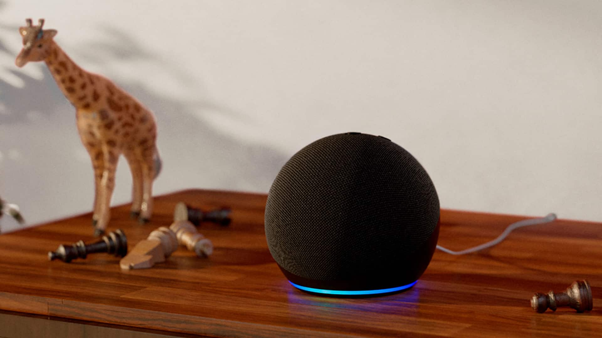
amazon echo dot gen 4
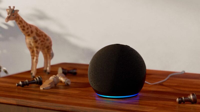
Enlarge / The 4th-gen Amazon Echo Dot smart speaker.

Alexa hasn’t worked out the way Amazon originally planned.

There was a time when it thought that Alexa would yield a robust ecosystem of apps, or Alexa Skills, that would make the voice assistant an integral part of users’ lives. Amazon envisioned tens of thousands of software developers building valued abilities for Alexa that would grow the voice assistant’s popularity—and help Amazon make some money.

But about seven years after launching a rewards program to encourage developers to build Skills, Alexa’s most preferred abilities are the basic ones, like checking the weather. And on June 30, Amazon will stop giving out the monthly Amazon Web Services credits that have made it free for third-party developers to build and host Alexa Skills. The company also recently told devs that its Alexa Developer Rewards program was ending, virtually disincentivizing third-party devs to build for Alexa.

Death knell for third-party Alexa apps

The news has left dozens of Alexa Skills developers wondering if they have a future with Alexa, especially as Amazon preps a generative AI and subscription-based version of Alexa. “Dozens” may sound like a dig at Alexa’s ecosystem, but it’s an estimation based on a podcast from Skills developers Mark Tucker and Allen Firstenberg, who, in a recent podcast, agreed that “dozens” of third-party devs were contemplating if it’s still worthwhile to develop Alexa skills. The casual summary wasn’t stated as a hard fact or confirmed by Amazon but, rather, seemed like a rough and quick estimation based on the developers’ familiarity with the Skills community. But with such minimal interest and money associated with Skills, dozens isn’t an implausible figure either.

Amazon admitted that there’s little interest in its Skills incentives programs. Bloomberg reported that “fewer than 1 percent of developers were using the soon-to-end programs,” per Amazon spokesperson Lauren Raemhild.

“Today, with over 160,000 skills available for customers and a well-established Alexa developer community, these programs have run their course, and we decided to sunset them,” she told the publication.

The writing on the wall, though, is that Amazon doesn’t have the incentive or money to grow the Alexa app ecosystem it once imagined. Voice assistants largely became money pits, and the Alexa division has endured recent layoffs as it fights for survival and relevance. Meanwhile, Google Assistant stopped using third-party apps in 2022.

“Many developers are now going to need to make some tough decisions about maintaining existing or creating future experiences on Alexa,” Tucker said via a LinkedIn post.

Alexa Skills criticized as “useless”

As of this writing, the top Alexa skills, in order, are: Jeopardy, Are You Smarter Than a 5th Grader?, Who Wants to Be a Millionaire?, and Calm. That’s not exactly a futuristic list of must-have technological feats. For years, people have wondered when the “killer app” would come to catapult Alexa’s popularity. But now it seems like Alexa’s only hope at that killer use case is generative AI (a gamble filled with its own obstacles).

But like Amazon, third-party developers found it hard to make money off Skills, with a rare few pointing to making thousands of dollars at most and the vast majority not making anything.

“If you can’t make money off it, no one’s going to seriously engage,” Joseph “Jo” Jaquinta, a developer who had made over 12 Skills, told CNET in 2017.

By 2018, Amazon had paid developers millions to grow Alexa Skills. But by 2020, Amazon reduced the amount of money it paid out to third-party developers, an anonymous source told Bloomberg, The source noted that the apps made by paid developers weren’t making the company much money. Come 2024, the most desirable things you can make Alexa do remain basic tasks, like playing a song and apparently trivia games.

Amazon hasn’t said it’s ending Skills. That would seem premature considering that its Alexa chatbot isn’t expected until June. Developers can still make money off Skills with in-app purchases, but the incentive is minimal.

“Developers like you have and will play a critical role in the success of Alexa, and we appreciate your continued engagement,” Amazon’s notice to devs said, per Bloomberg.

We’ll see how “critical” Amazon treats those remaining developers once its generative AI chatbot is ready.

https://arstechnica.com/?p=2016625


Apple will allow reuse of iPhone parts for repairs, with a notable catch

Technician repairing mobile phone at a station with microscope, heat gun, and blue mat
Getty Images

Apple has always had a strong preference that only its own parts be used in repairs, but only if they’re brand-new. Now, soon after Oregon passed a repair bill forbidding devices from rejecting parts with software locks, or “parts pairing,” Apple says it will allow for used Apple parts in future iPhone repairs.

While noting that “pairing” is “critical to preserving the privacy, security, and safety of an iPhone,” Apple states that it has worked for two years to allow for reusing Face ID and Touch ID sensors (i.e., biometric sensors) as well as moving part calibration from its remote repair certification tools onto the iPhone itself. As a result, “select iPhone models” this fall will allow for reusing biometric sensors and other parts, and anyone ordering parts from Apple can skip sending a device’s serial number, so long as the repair doesn’t involve a new main logic board.

The new policy “is designed to maintain an iPhone user’s privacy, security, and safety, while offering consumers more options, increasing product longevity, and minimizing the environmental impact of a repair,” according to Apple’s release.

“At Apple, we’re always looking for new ways to deliver the best possible experience for our customers while reducing the impact we have on the planet, and a key part of that means designing products that last,” John Ternus, Apple’s senior vice president of hardware engineering, said in a statement. “With this latest expansion to our repair program, we’re excited to be adding even more choice and convenience for our customers, while helping to extend the life of our products and their parts.”

Apple also announced that iPhones’ Parts and Service history will be expanded to show whether each part that has been replaced is a new or used Genuine Apple part. Apple did not mention aftermarket parts but will presumably continue to label those as an “Unknown Part.”

Activation Lock and e-waste

Apple’s proclivity for parts pairing has often been linked to the company’s concerns over reuse of parts from stolen iPhones. Apple acknowledges this by announcing the addition of what it terms its “popular Activation Lock feature” to parts themselves, aiming to deter stolen iPhones from being parted out. If a device is being repaired and detects that a part came from a device that had Activation Lock or Lost Mode enabled, it won’t let that part be calibrated.

Activation Lock has long been a major hindrance to anyone working to fix, refurbish, or rework Apple devices, by design or otherwise. Activation Lock was (as Apple notes) introduced in 2013 to appease lawmakers concerned about a growing trend of smartphone theft and was then expanded to other Apple products. But a substantial number of people do not deactivate Activation Lock before selling, recycling, or sometimes simply losing their device. If an original device owner cannot be reached (or motivated) to deactivate the lock from another device, an otherwise working iPhone, iPad, MacBook, or other Apple device can end up as a paperweight.

As noted by Vice and 9to5 Mac, this extends to perfectly usable M1 MacBooks from 2020, as well as entire fleets of corporate devices traded out without Activation Lock deactivated. Repair site iFixit considered the iPhone 14 and 15 to be some of the most repairable devices Apple has made in modern times but have lowered their scores for extensive failures after genuine parts swaps. Lidar sensors, the front-facing camera, auto brightness sensors, and more fail, and other parts issue warnings.

Apple’s new middle ground of using software locks to make stolen parts far less valuable or worthless but allowing genuine parts salvaged legitimately to be calibrated and functional would seem to be an improvement over certain Apple parts refusing to work anywhere else. But Activation Lock neglect could leave discarded devices still mostly useless, even for parts.

Notable timing

PIRG, the federation of state Public Interest Research Groups, pointed to not only the Oregon repair bill but also a similar bill in Colorado that has passed that state’s House and is due to be heard today in its Senate. “Make no mistake: The reason Apple is doing this is because Right to Repair is moving forward, thanks to the efforts of state lawmakers and our coalition of tinkers, fixers, makers and environmental and consumer advocates,” Nathan Proctor, senior director of PIRG’s right to repair campaign, said in a statement.

iFixit CEO Kyle Wiens also pinned Apple’s announcement to the Colorado bill. Wiens, who authored a blog post shortly after Apple’s announcement, described Apple’s new policy as “a strategy of half-promises and unnecessarily complicated hedges” designed to deflect more laws that would ban pairing entirely. “Aftermarket parts are key to the repair ecosystem, and Apple seems keen on continuing to ban those,” Wiens wrote to Ars.

Ars has reached out to Apple for comment and will update this post with new information.

Disclosure: Kevin Purdy previously worked for iFixit. He has no financial ties to the company.

This post was updated to link an iFixit blog post and note Apple’s language about “select iPhone models” eligible for used parts.

https://arstechnica.com/?p=2016470


Google Cloud rolls out self-designed Arm chips in its data centers

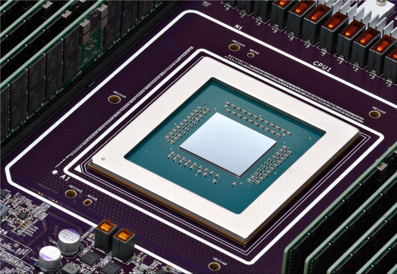
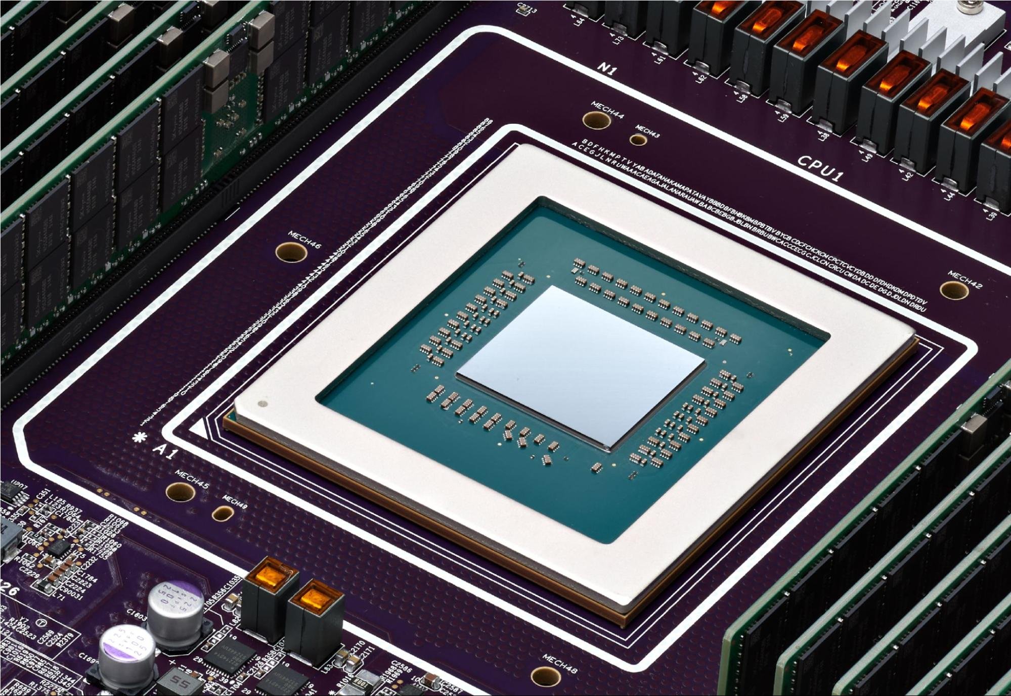
A Google Axion Processor.
Enlarge / A Google Axion Processor.

Google is joining the custom Arm data center chip trend. Google Cloud, the cloud platform division that competes with Amazon Web Services and Microsoft Azure, is following in the footsteps of those companies and rolling out its own Arm-based chip designs. Google says its new “Google Axion Processors” are “custom Arm-based CPUs designed for the data center” and offer “industry-leading performance and energy efficiency.”

Google has been developing custom data center accelerators for things like AI and video transcoding, but this is the first time the company is making a CPU. Google says it’s seeing “50% better performance and up to 60% better energy-efficiency than comparable current-generation x86-based instances.“

Google’s “Axion” chip is based on the Arm Neoverse V2 CPU, so just like the ARM chips we see on mobile devices, by making “custom” chips, these companies are closely following a lot of blueprints that Arm makes available. Google says it did include a custom microcontroller called “Titanium,” which it says handles networking, security, and storage I/O.

This is Google Cloud, so you won’t be buying anything with an “Axion” chip in it. You can pay for cloud processing that uses the new CPU, with Google naming “Google Compute Engine, Google Kubernetes Engine, Dataproc, Dataflow, Cloud Batch, and more” as services that will use the new chip. Some of these services bill by “vCPU” usage, so theoretically a faster CPU could lead to lower prices, but Google doesn’t spell that out in the post. Internally Google is also moving BigTable, Spanner, BigQuery, Blobstore, Pub/Sub, Google Earth Engine, and the YouTube Ads platform from its current Arm servers to this new custom one soon.

It’s a bit strange to tout a new cloud infrastructure CPU when the whole point of services like AWS and Google Cloud is that you don’t have to worry about the server. The services you were running will continue to run, while companies like Google, Amazon, and Microsoft can take care of all that complicated hardware and network data center stuff. Google says that Axion VMs will be available as a “preview” in “the coming months” and that Cloud customers can sign up for access.

https://arstechnica.com/?p=2016132


Fairbuds are Fairphone’s proof that we really could make better tiny gadgets

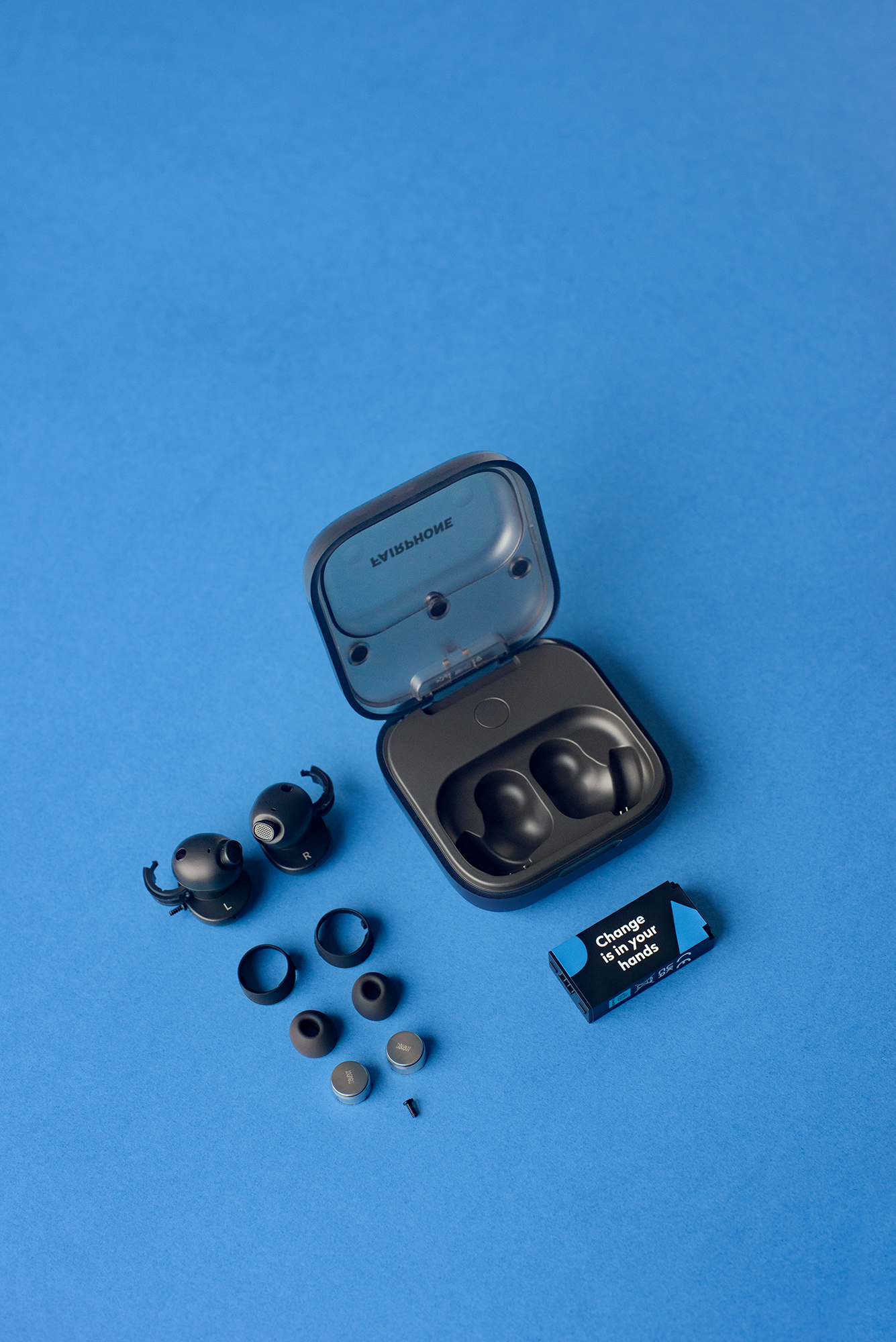
Fairbuds with all their components laid out on a blue background
Enlarge / The Fairbuds and their replaceable components, including the notably hand-friendly, non-soldered batteries.

Fairphone has spent years showing us that it could do what major phone manufacturers suggest is impossible: make a modern-looking phone, make it brazenly easy to open up, design it so battery swaps are something you could do on lunch break, and also provide software support for an unbelievable eight to 10 years.

Bluetooth headphones, specifically wireless earbuds, seemed destined to never receive this kind of eco-friendly, ownership-oriented upgrade, in large part because of how small they are. But the Fairbuds have arrived, and Fairphone has made them in its phones’ image. They’re only available in the EU at the moment, for 149 euro (or roughly $160 USD). Like the Fairphone 4, there’s a chance interest could bring them to the US.

The highlights include:

  • Seven replaceable parts from the buds and charging case, all sold by Fairphone
  • A two-year warranty, expanded to three if you register them
  • Batteries in both the case and buds that are replaceable
  • IP54 sweat and water resistance
  • Individual left or right buds and a charging case that Fairphone will sell to you
  • Made with “fair and recycled materials,” in “fair factories,” and “climate conscious and electronic waste neutral,” (as explained by Fairphone).

Of course, the buds also, you know, produce sound, with 11 mm titanium drivers. The Fairbuds sport active noise-canceling and ambient sound modes, Bluetooth 5.3 with “dual point connectivity” for quick-switching between devices, and a Fairbuds app for customizing EQ and preset settings. The buds’ 45 mAh batteries carry about six hours of listening per charge, and their 500 mAh case adds another 20 hours.

It’s not Fairphone’s first foray into fair, repairable sound devices. The firm previously made the since-discontinued True Wireless Stereo Earbuds and still offers Fairbuds XL, which are not buds at all but full over-ear headphones (and also EU-only).

The best that major-brand earbuds have ever done in repairability is “maybe you can do it, if you’re careful, and you don’t mind losing water resistance.” Taylor Dixon took apart six buds for iFixit back in 2020, and only Sony’s WF-1000XM3 didn’t require soldering, cutting and re-applying glue, and a steady hand working in very small spaces.

AirPods? AirPods are something else. One firm, The Swap Club, has figured out some means of getting the battery out of AirPods and selling them refurbished. But they only accept regular AirPods, not AirPods Pro. Alternatively, Apple will send you a pre-paid label to send in your spent AirPods for recycling, though with no trade-in credit. Even if Apple gets some kind of material out of the AirPods, a lot of them (and nearly every other wireless earbud) end up as waste after 18 months or however long their batteries last.

Fairbuds may or may not take a big chunk out of the market for AirPods, Beats, Pixel Buds, or other use-and-toss airbuds. But at a minimum, they give people something to point to as proof this category could be a lot better.

Disclosure: Kevin Purdy used to work for iFixit. He has no financial ties to the company.

Listing image by Fairphone

https://arstechnica.com/?p=2016094