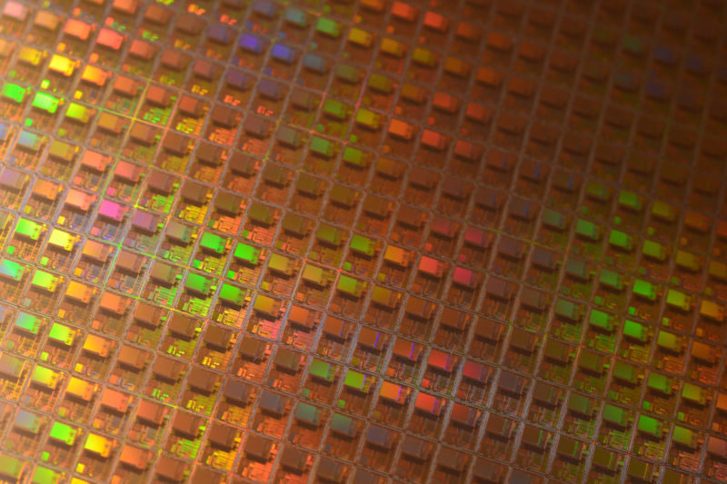
Chips built with extreme ultraviolet (EUV) light are plagued with random defects with no obvious solution, according to research presented at a chipmakers’ conference reported in EETimes. The EUV hardware seems to work acceptably for 20nm or larger processes, but below this scale, small defects are cropping up that ruin the chip and prove hard to detect.
Photolithography is the process used to etch the patterns that make up chips into a silicon wafer. The wafer is coated with a light-sensitive material called photoresist. This wafer is then exposed to bright light that’s shone through a mask. Areas hidden by the mask will retain their photoresist layer; those exposed directly to the UV will lose it. The wafer is then etched using plasma or acid. Parts of the wafer that are still covered in photoresist are protected during the etching, retaining their silicon oxide; those whose photoresist has been removed are etched away.
Smaller wavelengths of light enable finer detail in the mask and hence finer detail in the etching. Processors today, built on a 14nm process, already use features that are far smaller than the wavelength of regular UV light; they apply techniques such as multi-patterning (in which multiple masks and light exposure stages are used) to reach ever smaller sizes. These additional steps increase manufacturing time and error rates, hence the interest in shorter wavelengths. With EUV, smaller chip features could be produced without needing such techniques.
The chip-building industry has been talking about using EUV photolithography—light with a wavelength of 13.5nm, compared to the 193nm ultraviolet in use today—since the late 1990s. In theory, EUV should make it easier to build processors with smaller features—narrower wires, tinier transistors—but getting EUV to work has proven problematic. EUV is strongly absorbed by air and by the materials used to make lenses; it can still be focused and redirected, through the use of mirrors rather than lenses. Efficient generation of high-intensity EUV has also been difficult. Commercial applications need at least 250W light sources, with Intel claiming it needs as much as 1kW.
GlobalFoundries, Samsung, and TSMC have all outlined plans to use 250W EUV sources for 7nm manufacturing. This is at the level that researchers are seeing problems. These problems include both areas where not enough material is etched away, causing shorts between wires in the chip, and areas where too much is etched away, causing gaps and tears in things that should be continuous.
GlobalFoundries VP of Research George Gomba described similar defect problems with EUV and said that the EUV hardware—the NXE-3400 from ASML—wasn’t yet up to the standard the company needs. He also said that better systems for inspecting the EUV masks are needed. Research is also needed to improve the photoresists, to understand their behavior when exposed to EUV and reduce the number of defects.
If these problems can’t be ironed out, they may force a different approach to chip design. Chips that combine memory with processing elements and chips based on neural networks are more resilient to manufacturing defects, as the individual bad elements can be disabled while still salvaging the chip as a whole. IBM’s True North neuron-simulating processor has a grid of 4096 elements, each combining some memory with some compute power, and last week researchers published that they had built “memtransistors.” These combine transistors with memristors (devices that change their resistance depending on their “memory” of how much electric charge has passed through them). These hybrids integrate computation and memory at a very low level.
https://arstechnica.com/?p=1266603

