-
This slide from IBM’s preview announcement gives more detail on the new process design.
-
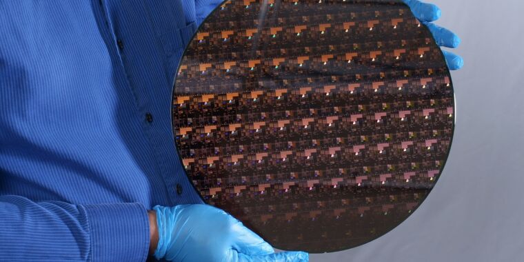
This wafer contains hundreds of simple prototype chips built on the new 2 nm process at IBM’s Albany research plant.
-
Transmission electron microscopy gives us a detail of the triple-stack GAA (Gate-All-Around) transistors in the new process.
On Thursday, IBM announced a breakthrough in integrated circuit design: the world’s first 2 nanometer process. IBM says its new process can produce CPUs capable of either 45 percent higher performance or 75 percent lower energy use than modern 7 nm designs.
If you’ve followed recent processor news, you’re likely aware that Intel’s current desktop processors are still laboring along at 14 nm, while the company struggles to complete a migration downward to 10 nm—and that its rivals are on much smaller processes, with the smallest production chips being Apple’s new M1 processors at 5 nm. What’s less clear is exactly what that means in the first place.
Originally, process size referred to the literal two-dimensional size of a transistor on the wafer itself—but modern 3D chip fabrication processes have made a hash of that. Foundries still refer to a process size in nanometers, but it’s a “2D equivalent metric” only loosely coupled to reality, and its true meaning varies from one fabricator to the next.
To get a better idea of how IBM’s new 2 nm process stacks up, we can take a look at transistor densities, with production process information sourced from Wikichip and information on IBM’s process courtesy of Anandtech‘s Dr. Ian Cutress. Cutress got IBM to translate “the size of a fingernail”—enough area to pack 50 billion transistors using the new process into 150 square millimeters.
| Manufacturer | Example | Process Size | Peak Transistor Density (millions/sq mm) |
| Intel | Cypress Cove (desktop) CPUs | 14 nm | 45 |
| Intel | Willow Cove (laptop) CPUs | 10 nm | 100 |
| AMD (TSMC) | Zen 3 CPUs | 7 nm | 91 |
| Apple (TSMC) | M1 CPUs | 5 nm | 171 |
| Apple (TSMC) | next-gen Apple CPUs, circa 2022 | 3 nm | ~292 (estimated) |
| IBM | May 6 prototype IC | 2 nm | 333 |
As you can see in the chart above, the simple “nanometer” metric varies pretty strenuously from one foundry to the next—in particular, Intel’s processes sport a much higher transistor density than implied by the “process size” metric, with its 10 nm Willow Cove CPUs being roughly on par with 7 nm parts coming from TSMC’s foundries. (TSMC builds processors for AMD, Apple, and other high-profile customers.)
Although IBM claims that the new process could “quadruple cell phone battery life, only requiring users to charge their devices every four days,” it’s still far too early to ascribe concrete power and performance characteristics to chips designed on the new process. Comparing transistor densities to existing processes also seems to take some of the wind from IBM’s sails. Comparing the new design to TSMC 7 nm is well and good, but TSMC’s 5 nm process is already in production, and its 3 nm process, which has a very similar transistor density, is on track for production status next year.
We don’t yet have any announcements of real products in development on the new process. However, IBM currently has working partnerships with both Samsung and Intel, who might integrate this process into their own future production.
Listing image by IBM
https://arstechnica.com/?p=1763407

